Innosilicon T1/T2 Hash Board Repair Manual
Mainly describes how to troubleshoot various faults of the Innosilicon T1 T2 computing board, and explains how to use the test fixture sold by ThanosMining for accurate positioning.
New version of test fixture: Innosilicon test fixture
Scope: applicable to all T1 production, after‑sales, and outsourcing maintenance sites
1. Maintenance platform requirements:
Constant temperature soldering iron ( 350 Degree‑‑ 400 Degrees), the pointed soldering iron tip is used for soldering small patches such as chip resistors and capacitors. 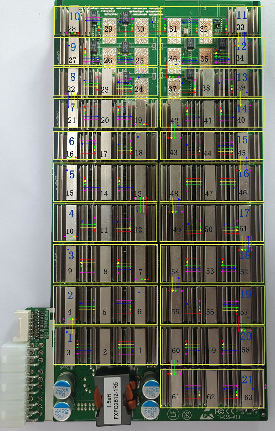
figure 1
Test whether the SPI waveform of the error‑reporting chip is normal; the picture above is the PCB board SPI Trend and voltage domain and chip sequence bit number
1. Each yellow box in the figure is a voltage domain, a total of twenty one Voltage domains, each voltage domain is on average 0.42V
2. The black numbers represent the order and bit number of the chip
3. The red arrow in the figure shows CLK Signal direction
The yellow arrow shows the direction of the SCK signal;
The green arrow shows the direction of the CS signal;
The blue arrow shows the direction of the DI signal;
The purple arrow shows the direction of the DO signal.
4. There is between every two chips 1‑7 Test point 1 for CLK Signal; test point 2 for RST Signal; test point 3 for EN Signal; test point 4 for SCK Signal; test point 5 for CS Signal; test point 6 for DI Signal; test point 7 for DO signal.
DI signal flow direction, from No. 63 chip to 1 Return the chip number, and then return to the control board;
DO signal flow direction, by 1 No. chip pulls low level toward 63; not plugged in IO Line, standby 0V , When calculating 0.3 Pulse signal around.
The RST signal flows in from the control board, and then by 1 Chip to 63 No. chip transmission.
2. The figure below shows the key circuits on the front of the T1 arithmetic board. 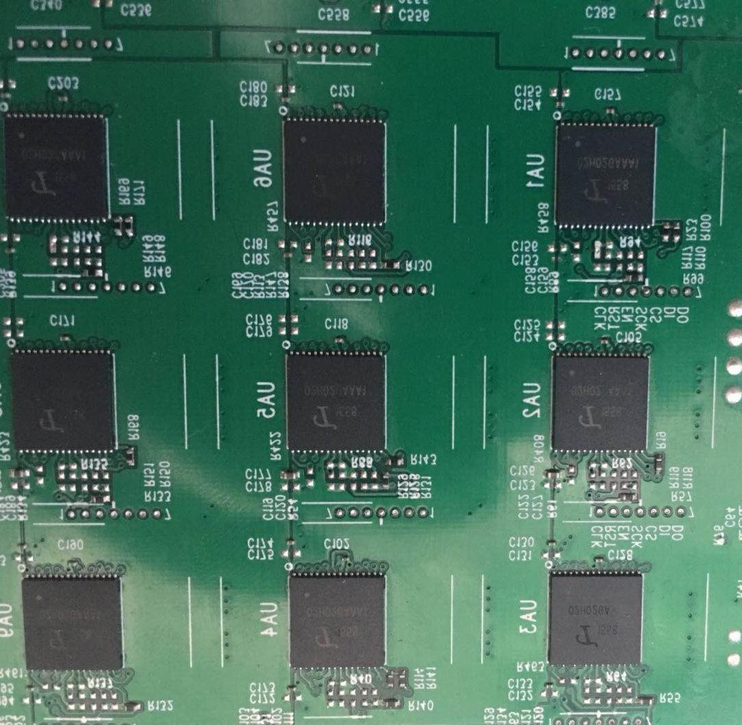
2 figure 2
1). Test points between each chip (as shown in the figure after zooming in): Figure 2
Figure 2. When repairing test points between chips, the test points between test chips are the most direct fault location
2) Voltage domain: The whole board has 21 voltage domains, and each voltage domain has 3 chips. The three chips in the same voltage domain are powered in parallel, and then connected in series with other voltage domains after being connected in parallel. The circuit structure is shown in Figure 4 below:
Principle analysis of voltage domain single chip (see Figure 3 below) 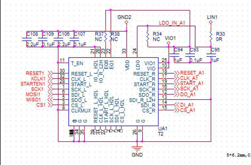
figure 3
● The above are the functions of each pin of the T1558 chip.
During maintenance, 14 test points before and after the chip are mainly tested (seven points before and after the chip: CLK , RST, EN , SCK, CS, DI, DO); DCDC Voltage output 8.82V;, boost voltage 11V, LDO‑‑1.8V, etc.
Detection method: 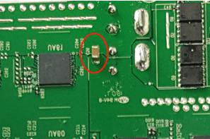
figure 4. The two ends of the C56 capacitor are the total DCDC output voltage, which should be about 8.82V
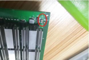
figure 5. Both ends of the C57 capacitor are the boost voltage, which should be about 11V
Figure 6. BM1558 circuit diagram
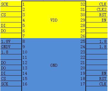
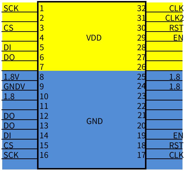
Figure 7. BM1760 chip pins
CLK: 0.9V provided by Y1 12M crystal oscillator
DO: From the first chip to the last chip provided by the control board, the signal can be measured with an oscilloscope
DI: Return from the last chip to the first chip, the signal can be measured with an oscilloscope
SCK: When the control board provides about 0.12V for calculation, the abnormal or low voltage will cause the calculation board to be abnormal or the calculation power is low
EN: 1.8V Provided by the control board
CS: Provided by the control board
RST: 1.8V . Provided by the control board, each time the test key is pressed, a low‑level reset signal will be output again.
When the above‑mentioned test point status and voltage are abnormal, please estimate the fault point based on the circuit before and after the test point.
It can be seen from the chart above:
CLK signal: by the chip 32 Or 31‑pin in, 17‑pin out, when connected across the voltage domain, by 5 Foot out through 100NF The capacitor is connected to the input to the next chip twenty three foot.
DO signal: enter from pin 6 of the chip, 12 Foot out
DI signal: returned by the chip from pin 5, output from pin 13 or 14;
CS signal: input from pin 3 of the chip and output from pin 15;
RST signal: by the chip 30 Foot in, 118 Pin output.
Test the signal voltage of each chip, LDO‑1.8OV
CORE: 0.8V‑‑‑ When this voltage is abnormal, it is usually the chip of the voltage domain CORE Short circuit
LDO‑1.8O: 1.8V‑‑‑‑ When this voltage is abnormal, the chip LDO‑1.8O Short circuit or open circuit
3) Judging the operating status of the computing board, the computing capability of the chip, and the temperature sensitivity based on the information in the printing window of the manufacturing tool.
3. O IO Definition
IO is composed of 2X7 pitch 2.0 PHSD 90 degree in‑line double row. 
The pin definitions are shown in Figure 8 below:
As shown in FIG:
1 pin is LED
2 feet for VIDD
10.14 Feet: for GND .
3 feet are EN
4 feet for STAR
Pin 7 is PLUG
12 feet for SCK
13 feet are CS
8.9 Feet (DI, EO)
6 feet ( RST ): is the reset signal 3.3V Terminal, after being divided by resistors, it becomes 1.8V RST Reset signal.
5 feet ( 3V3 ): is the computing board 3.3V Power supply, the 3.3V Provided by the control board, mainly for PIC Provide working voltage.
TX_IN voltage is 1.8V
RST_IN voltage is 1.8V
4. Routine maintenance process:
● Reference steps:
1. Routine inspection: First, perform visual inspection on the arithmetic board to be repaired to observe whether there is any displacement, deformation, or scorching of the small heat sink? If any, you must deal with it first; if the small heat sink is displaced, remove it first, wash off the original glue, and re‑adhesive after the repair is passed.
Secondly, after the visual inspection is no problem, the impedance of each voltage domain can be tested first to detect whether there is a short circuit or an open circuit. If you find out, you must deal with it first.
Thirdly, check whether the voltage of each voltage domain reaches 0.42, and the voltage difference of each voltage domain shall not exceed 0.05V . The voltage of a certain voltage domain is too high or too low
Yes, the circuits in the adjacent voltage domains generally have abnormal phenomena. Need to investigate the reason first.
2. After the routine detection is no problem (generally, the short‑circuit detection of the routine detection is necessary, so as not to burn the chip or other materials due to the short circuit when the power is turned on), you can
Use DEBUG connection for chip detection, and judge and locate according to the detection result.
3. According to the display results of the test and detection, starting from the vicinity of the faulty chip, check the chip test points (CLK, RST, EN,
SCK, CS, DI, DO); DCDC voltage output 8.82V; boost voltage 11V, LDO‑‑ 1.8V etc.
4. Divide according to the signal flow direction DI Signal reverse transmission ( 6 To 1 Number chip), several of which signal CLK , RST , EN , SCK , CS ,, DO Is forward pass ( 1‑63 ), find the abnormal fault point through the power supply sequence.
5. When locating the faulty chip, the chip needs to be welded again. The method is to add flux around the chip (preferably no‑clean flux), and then insert the chip
When the solder joints of the pins are heated to a dissolved state, gently move up, down, left, and right to press the chip; the chip pins and the pads are re‑melted and the tin is collected. To achieve
The effect of tin is renewed. If the fault remains the same after re‑soldering, you can directly replace the chip.
6. The repaired computing board must be tested twice or more during testing. Two test times before and after: the first time, after the replacement of parts is completed, it is necessary
After the arithmetic board has cooled down and passed the test, put it aside first. For the second time, after a few minutes wait for the arithmetic board to cool down, test again. Although twice
The test time is a few minutes, but this does not affect the work. Put the repaired board aside, continue to repair the second board, wait for the second board to be repaired and placed
While cooling, test the first piece. In this way, the time is just staggered, and the total time is not delayed.
7. The repaired board. It is necessary to classify the faults and make records of the type, location, reason, etc. of the replacement components. For feedback back to production and after‑sales, Research and development.
8. After recording, install it into a complete machine for formal aging.
Five failure types:
1. The impedance of each voltage domain is unbalanced; when the impedance of some voltage domains deviates from the normal value, it indicates that there are parts in the abnormal voltage domain that have open circuits and short circuits. The most likely cause is the general chip. But there are three chips in each voltage domain, and often only one has a problem when it fails. Find out the problem chip
The method can detect and compare the test points of each chip to the ground impedance to find the abnormal point. If you encounter a short circuit, you can first use the same voltage on the chip.
Remove the hot plate first, and then observe whether the chip pins are connected to tin. If the short‑circuit point cannot be found in the appearance, you can find the short‑circuit point according to the resistance method or the current cut Waypoint.
2. Unbalanced voltage in the voltage domain;
When the voltage of some voltage domains is too high or too low, it is generally due to the abnormal voltage domain or the signal abnormality in the adjacent voltage domain, which leads to the following or down
A voltage domain works abnormally and the voltage is out of balance. Only by detecting the signal and voltage of each test point, the abnormal point can be found.
Compare the impedance of the test point to find out the abnormal point.
Observe the appearance, measure the impedance, measure the voltage, and detect the voltage and power supply of each test point. The test locates the chip according to the detection information, first re‑soldering, re‑soldering is invalid, replace it with the fault type record and test more than two times Ok can be considered as repaired Ok and then carry out related aging
Pay special attention to the fact that the CLK signal and RST Signal, these two abnormalities are most likely to cause voltage imbalance.
3. Lack of chip; Lack of chip means that the test box cannot detect all of them during testing. 63 For each chip, it is often impossible to detect as many chips as they actually are. However, the actual missing (undetected) abnormal chip is not in the displayed position. At this time, it is necessary to accurately locate the abnormal chip through testing.
The positioning method can use TX cut‑off to find the position of the abnormal chip. Is to convert a certain chip TX Signal to ground, for example: connect the first 50 Chip TX Output the ground of the voltage domain
After that, in theory, if all the previous chips are normal, 50 chips should be detected in the test box? If not detected 50 Chips, indicating that the abnormality is in the 50 Chip before; if 50 chips are detected, it means that the abnormal chip is after the 50th chip. By analogy, use dichotomy to find the location of the abnormal chip.
4. Broken link;
The broken link is similar to the lack of a chip, but the broken link does not mean that the chips that cannot be found are abnormal, but the abnormal chip behind the abnormal chip is caused by the abnormality of a certain chip.
All chips fail. For example, a chip itself can work, but it will not forward other chip information; at this time, the entire signal chain will suddenly stop here.
However, losing a large part of it is the broken link. Generally, the broken link can be displayed in the test box, for example: when the test box is testing the chip,
Only 14 chips are detected. If the preset number of chips is not detected in the test box, it will not run, so it will only display how many chips are detected.
At this time, just check the voltage and impedance of each test point before and after the 14th chip according to the displayed number «14» to find the problem.
5. Not running;
Not running means that the chip information of the arithmetic board cannot be detected in the test. E0:1 is the most common phenomenon, and the range of faults involved is wider.
1) Non‑operation caused by abnormal voltage in a certain voltage domain; the problem can be found by measuring the voltage of each voltage domain.
2) The abnormality caused by a certain chip abnormality can be found by measuring the signal of each test point.
CLK signal: the signal is generated by 1 No. chip output to 63 No. chip, but the current version has only two crystal oscillators, Y1(1‑30)X1(31‑63) of which as long as there is an abnormal signal clk Yes, all the following signals will be abnormal, search in order according to the signal transmission direction.
DO signal: This signal is caused by 1 , 2 , 3 . 63 No. chip, when a certain point of the dichotomy is abnormal, it can be detected forward.
DI signal: This signal is caused by 63.60 , 59, 58, ,, 1 If the number returns, confirm the cause of the fault through the chip signal trend,
The signal is the highest priority if the T1 operation board is not running, and the signal is searched first.
RST signal: 1.8V ; After the arithmetic board is powered on and the 14P signal is plugged in, this signal will change from 01 , 02,, 0 63 The direction of the transmission to the last chip.
3) A certain chip VDD It can be caused by measuring whether the potential difference of each voltage domain is normal. Under normal circumstances, when the VDD voltage is 0.42, the normal voltage of each test point in other voltage domains is also 0.42 to ensure the balance between the voltage domains.
4) of a certain chip VDD1V8 Abnormal voltages Determine whether a certain VDD1V8 voltage is normal by measuring the test points of each voltage. Generally, the LDO voltage determines the voltage of each test point. When the LDO voltage is 1.8V, the normal voltage of each test point in other voltage domains is also 1.8. V
5. Low computing power;
Low computing power can be divided into:
1) During the test, received Nonce Insufficient, lack of computing power and show bad phenomena. This phenomenon can be judged by seeing the number of nonce returned by each
chip directly through the serial port printing information. Generally, the chip with the returned nonce number lower than the set value should be trouble‑shooted, and the non‑welding and external causes can be directly replaced. .
2) During the test of the test box, the computing power is low after the whole machine is installed. Most of this situation is related to the heat dissipation conditions of the chip, so special attention is required
The small heat sink of each chip is glued, and the ventilation performance of the whole machine. Another reason is that the voltage of a certain chip is critical. After the whole device is installed, the 12V power supply and
The difference in the power supply during the test leads to a deviation between the test hashrate and the running hashrate. You can use the test box to test after turning it down, and adjust the voltage slightly. DC adjustable power supply
After the 12V output, the chip is tested again to find the voltage domain with the lowest number of returned nonces.
6. A certain chip NG ;
Refers to when the test is passed, the test serial port information shows that the returned nonce of a certain chip is insufficient or zero. In addition to eliminating the problem of false soldering and peripheral components, you can
Replace the chip directly.
● Maintenance instructions:
1. During maintenance, the maintenance personnel must be familiar with the function and flow direction of each test point, the normal voltage value and the ground impedance value.
2. Must be familiar with chip soldering, so as not to cause PCB Foaming deformation or damaged pins.
3. T1558 chip package, both sides of the chip 16 foot. The polarity and coordinates must be aligned during welding, and they must not be misaligned.
4. When replacing the chip, the thermal conductive adhesive around the chip must be cleaned to avoid IC Hanging or poor heat dissipation during soldering may cause secondary damage to the chip.
Innosilicon T2T-25T, -29T, T2TH, T2TZ, 30-37 Th/s

Все полезные ссылки и FAQ можно найти в первом сообщении. Прежде чем задать вопрос, посмотрите там.
Рекомендуемые сообщения
Для публикации сообщений создайте учётную запись или авторизуйтесь
Вы должны быть пользователем, чтобы оставить комментарий
Создать учетную запись
Зарегистрируйте новую учётную запись в нашем сообществе. Это очень просто!
Войти
Уже есть аккаунт? Войти в систему.
Последние посетители 0 пользователей онлайн
- Ни одного зарегистрированного пользователя не просматривает данную страницу
Similar Topics
Ремонт innosilicon a4+/a6
Innosilicon A10,- pro, 500 Mh/s, Ethereum
Innosilicon A11
10 Jan 2022, 15:07 в Прошивки
Innosilicon A4+ LTC Master
Ремонт innosilicon a4+/a6
- Ответов 431
- Создана 11 Oct 2019, 09:20
- Последний ответ 27 Jun 2023, 14:01
Топ авторов темы
sansche 36 постов
scopus 26 постов
hustle88 26 постов
iln5317 22 постов
Популярные дни
Популярные посты

Комрад
11 Oct 2019, 10:10
хочешь загубить аппарат-подключи к найсу. Найс-это не пул, а агрегатор мощностей.
12 Jul 2021, 02:43
Ищи в телеграмм N0TScrooge или cubich они умеют это лечить.
Onoprienko Bogdan
24 Nov 2021, 05:33
Понимаю что поздно, но все же. Тоже столкнулся с такой проблемой. Купил 4 т2т 25тх. Как полагается разобрал, почистил, три собрал обратно. Включаю первый, а там вечный тюнинг. Через /error 0 информаци
Innosilicon T2T model hash board repair guide
In the process of manufacturing and using the miner, if the user encounters chain loss, low hashrate, multiple hardware errors, etc., please refer to this manual for test and maintenance.
Note: This manual cannot cover all possible abnormal problems. If you encounter a problem that cannot be solved using this manual, please consult our relevant personnel, and they will update this manual when necessary.
Ⅰ. Overview
1. The circuit layout of the hash board and the distribution of test points
Take 3*31 model as an example. For other models, please refer to relevant design documents.
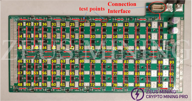
(1) The three adjacent chips in the figure are a voltage domain [(1,2,3), (4,5,6). (91,92,93)]. There are a total of 31 voltage domains on this hash board, and the voltages of the three chips in each voltage domain are the same, and the average voltage of each voltage domain is about 0.45V at startup (T series machines)
(2) The red arrow in the figure shows the transmission direction of CLK and communication signals;
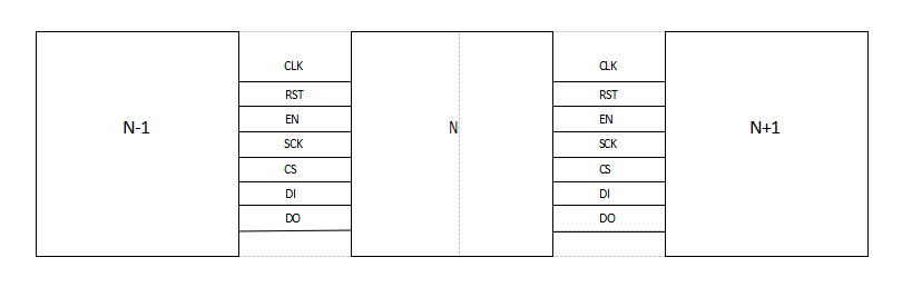
(3) There are 1 to 7 test points between each two chips (each model is different, please refer to the design file for details); test points 1 to 7 are CLK, RST, EN, SCK, CS, DI and DO signals respectively. Specifically as shown below:
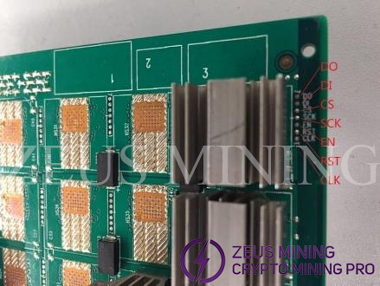
(4) Test points and connections between adjacent chips:
2. Description of the test software
After SMT, before sticking heat sink
It is used to quickly check soldering problems. It does not do a long time function test, but only tests whether the transmission of all chips is normal.
After pasting the heat sink on the non-chip side
It is used to check various faults of the single board in the high power state as early as possible. Due to the lack of a heat sink, the operating frequency of the chip is lower than that of normal use.
Binning after pasting
After all heat sinks are pasted
The test is carried out under 4 kinds of working voltages, and the boards are graded according to the measured hash rate. Boards of the same grade are loaded into a machine.
Locating problems with a single hash board
The program will send communication commands indefinitely for maintenance personnel to use multimeters and oscilloscopes to check the necessary circuits.
The machine is aged before leaving the factory
Use the official factory firmware, if there is an exception, an error code will be displayed on the mass production management interface.
3. Error code list of test software before and after pasting
If no problem is detected, "√" will be printed at the end of the log, otherwise it will be printed "×"。 When a problem is detected, the software will report the error type with the highest priority. The order of error priority is: E0>E9>E6>E4>E7>E5>
E3 > E1 > E2 > E8. The chip can be repaired or replaced according to the report.
Cannot find chip type
The number of good cores of a single chip is less than 30%
Statistics under operating frequency
The number of good cores of a single chip is less than 90%
Statistics under operating frequency
The single chip job test is all wrong
The PLL with the chip is not locked
The temperature of the chip is abnormal
9999 or — 9999 is displayed in the software
The voltage of the chip is abnormal
There is an error in the return process of the command, or the frequency increase fails
“E7:0” indicates that pll configuration failed
The total error rate of job testing of the whole board is greater than 10%
The number of chips read is wrong
Unable to find a suitable grade after pasting the heatsink
CRC error returned by the command
Failure to depressurize
4. Error code list of aging software
Methods of resolution
The IO of the control board is abnormal
Change the control board
The factory settings must be restored after completion
Network fault of control board
Hash board is failure
Change the hash board
After replacement, be sure to restore factory settings or re-aging after completion
The temperature of individual chips is too high
Change the power supply
It is recommended to restore factory settings or re-aging after completion
SPI line interference
Use shield wire
SPI cable is not plugged properly
Check and re-plug SPI flat cable
The power consumption of the whole machine is too high
Re-aging or frequency reduction (Efficiency mode)
The ambient temperature is too high
Check and re-plug SPI flat cable
Improve the operating environment
Check the fan cable connection / check whether the fan model matches / check whether the fan installation direction is correct
Reference document “Summary of Frequently Asked Questions about the Control Board”
Mining pool settings error
Check pool settings or restore factory settings
The network cable is not plugged properly
Check the network cable connection
Network environment failure
Check the DHCP and DNS configurations of the switch
One or more hash boards are not detected
The number of hash boards that have been detected. If there are more than one, separated by spaces
SPI cable not plugged in / IO fault of control board / Hash board fault
I2C communication of power supply is abnormal
PSU failure / Control board IO failure
All hash board encore failure
Control board IO failure / PSU failure / hash board failure
Partial hash board encore failure
The number of the normal encore hash board, if there are more than one, separated by spaces
Hash board failure / control board IO failure / PSU failure
Hash board number: wrong frequency point
SPI line interference / hash board failure
Failed to set voltage
Hash board No.: 1/2
SPI line interference / hash board failure
Hash board No.: 1/2
SPI line interference / hash board failure
SPI error cannot be recovered automatically at runtime
Hash board number
SPI line interference / hash board failure / control board IO failure
I2C communication fails during operation and cannot be recovered automatically
PSU failure / control board IO failure
Unable to connect to the mining pool
Mining pool setting error / network cable not plugged in properly / network failure of the control board / network environment failure
Individual chips are damaged, resulting in falsely high hashrate.
Damaged chip number: hashboard number. If there are more than one, separated by spaces
Hash board number
The ambient temperature is too high / fan failure / the temperature of individual chips is too high / the power consumption of the whole machine is too high
Failed to read temperature
Hash board number
Control board IO failure / hash board failure
SPI cable connection is abnormal
Hash board number
SPI port of the control board is inserted incorrectly / control board IO failure
Insufficient power supply
The number of good cores of the chip is abnormal
Hash board number: chip number
Hash board failure
Wrong vid type of control board
vidtype, minertype, subtype, chipnum
Hash board failure
II. Preparation of maintenance platform
Tools:serial port board / data cable / TF card / jumper cap / oscilloscope / multimeter
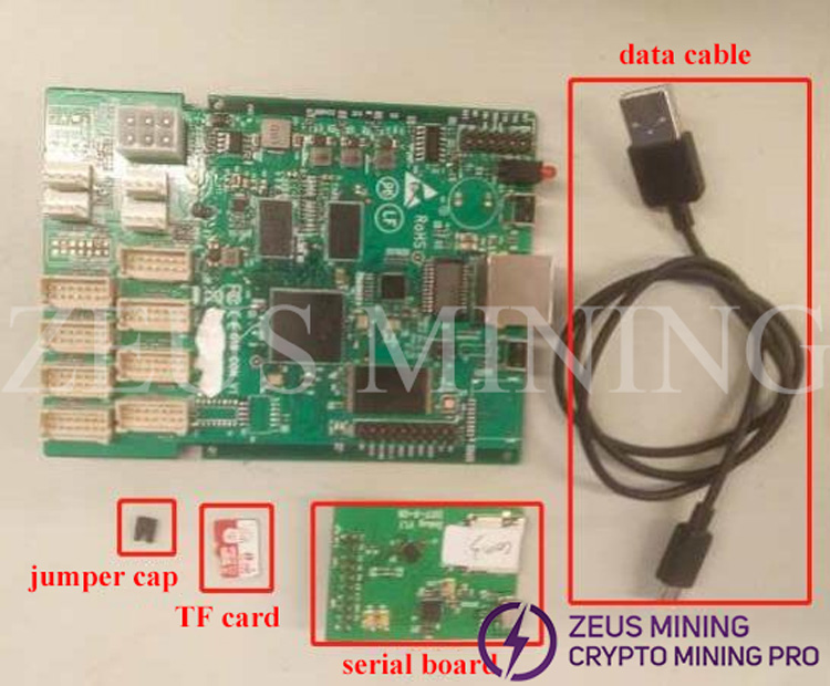
1. Software instructions
(1) Instructions for the test software *. bin
How to use: After shutting down, copy xxx.bin directly to the TF card, and insert the TF card into the slot of the serial port board. Then connect the serial port board to the control board, and use a jumper cap to connect to the J2 interface. Finally, boot it up.
(2) Instructions for the the serial port tool
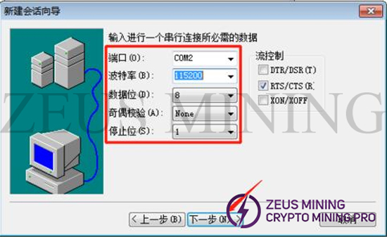
Install the serial port test tool (SecureCRT.exe) on the computer, and set the baud rate: 115200, n, 8, 1.
The setting method is as follows:
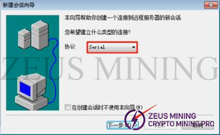
Double-click the serial port icon to open the serial port tool as shown in the figure below, click "New Dialogue" in the red box in the dialog box.
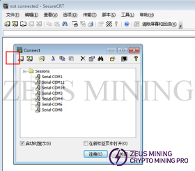
Select the serial in the New Session Wizard.
Set baud rate: 115200 and other options.
(3) Software instructions
① Software before and after pasting
The usage process is:
1) After inserting the SD card into the slot, check that the device is correct and power on.
2) Open the serial port software to check whether the software version information is correct after power-on.
3) During the test, the test information of each stage and other prompt characters will be displayed to facilitate hardware testing and status monitoring.
4) After the test is finished, print the test result. If it is a multi-chain test, the test results will be printed together after the test is finished.
5) To test again, directly press the reset key on the control board or press the enter key according to the prompt characters of the software.
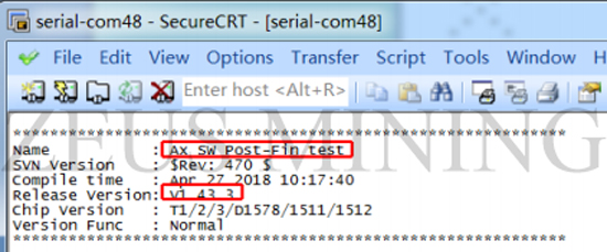
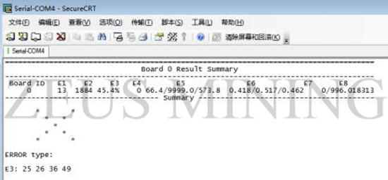
1) After inserting the SD card into the slot, check that the device is correct and power on.
2) Open the serial port software to check whether the version information of the software is correct after power-on.
3) During the test, the test information and LED lights of each stage will be displayed to facilitate hardware testing and status monitoring.
4) The software will continuously send a fixed command during operation, which can be used to measure voltage and signal.
5) After the measurement is completed, press the function key to continue running, and finally print the test results.
6) To test again, directly press the reset button on the control board or press the Enter button according to the characters prompted by the software.
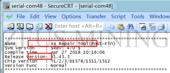
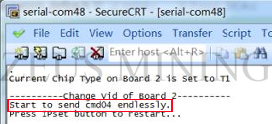
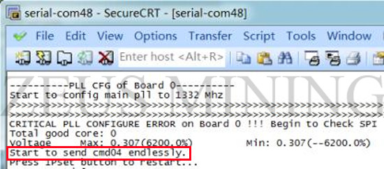
It should be noted that the maintenance software can only test one circuit board at a time. When the function key is pressed, only when the corresponding indicator light goes out can it be ensured that the key is successfully captured.
2. Establish a test environment
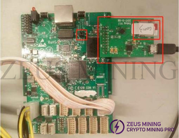
Take out the control board of the miner to be tested, place the control board and the serial port board as shown in the figure, insert the TF card, and insert the jumper cap into the J2 interface. Connect the serial port board and the computer with a data cable.
III. Maintenance process
1. The basic process of repairing the aging of the whole miner
(1) Reproduce the bad aging problem and record the error code. If you need our company's research and development analysis, you also need to save the aging log.
(2) Check whether the power output corresponding to the defective board is normal.
(3) If it is a multi-channel control power supply, exchange the power channel of the bad board and the normal board (note that the order of the data line interface is adjusted at the same time), and then observe whether the bad phenomenon follows the hash board or the power supply. If it follows the power supply, replace the power supply again. do aging.
(4) Disconnect the power supply and network cable. Check whether the appearance of the machine is damaged. Check whether the power and data cables are loose or disconnected.
(5) Use the original machine power supply and the faulty hash board to do a sticky test in the bucket, and record the error code and log. If there is no abnormality after 5 consecutive tests, our R&D personnel will be notified for analysis.
(6) Use the original machine power supply and the faulty hash board, and do a post-stick test outside the barrel to see if the phenomenon still exists and make a record. If the chip surface is a heat sink fixed by screws, remove the heat sink on the chip surface, and then do a pre-stick test to see if the phenomenon still exists, and make a record.
(7) Continue to analyze in accordance with the faulty board repair process.
2. The basic process of repairing the single board
Before maintenance, please confirm that the power supply, control board, and various cables are connected properly.
(1) Use the pre-glue test software to test and get the error code Ex:x. Different next steps may be taken for different types of errors.
(2) Check the appearance of the board, and observe whether there are missing components, errors, or abnormal appearance. Check whether there are solder balls, foreign objects, etc. near the error chip.
(3) Run the maintenance procedure and check the input voltage with a multimeter. Check crystal oscillator supply. Check tail IO boost circuit. Check the LDO output of each stage.
(4) Use an oscilloscope to check the chip input and output signals CLK, SCK, DO, DI, CS, RSTN, START.
(5) If the output signal of the ASIC chip is found to be abnormal, do not easily replace the chip. According to the instructions in the following chapters, first try methods such as adding soldering, re-soldering, and swapping with other chips on this board.
(6) If the method of chip exchange is adopted, it can be observed whether the problem follows the chip.
(7) If the above method is invalid, then replace the chip. It is necessary to record in detail the specified information such as the cause of the problem of the removed chip in the maintenance report. Regularly send the maintenance report to our company for analysis.
3. Locate the broken chain with a maintenance-specific program
Copy the provided repair.bin to the TF card and plug it into the serial board. Connect power and data cables (no fan required), power on. According to the error message of the software before or after gluing, detect the test points of the relevant chip and its adjacent chips.
Description of function keys and indicators in the service software.
(1) After power on, the lights on the control board are on (red and green lights next to the reset button). If the power-on link is broken, the software will keep sending cmd04. After pressing the function key next to the USB card slot, the software will stop sending cmd04, and the program will continue to run, and the green light will be off at this time;
(2) If the power-on link is connected, the software will continue to send cmd04. Similarly, after pressing the function key, it will stop sending cmd04, and then the green light will go out;
(3) After the frequency configuration fails, the software will send cmd04 at the point of failure, press the function key, stop sending cmd04, the program continues to run, and the red light is off at this time;
(4) After the frequency configuration is successful, if the link breaks during the continuous reading process, the software will send cmd04 at the link break. After pressing the function key, the transmission will stop, and the red light will be off at the same time, and the program will continue to execute.
IV. Analysis of typical problems
1. E0: 1
This kind of problem is that the communication chain is completely broken, and most of them are caused by abnormal peripheral circuits. Known causes are:
(1) The power supply has no output or the output is abnormal.
(2) The solder connection between the communication interface and the plug-in pin is shorted.
(3) The data cable is not plugged in properly or the contact is poor or damaged, resulting in a short circuit.
(4) The components between the communication interface and the first chip have problems such as false soldering, short circuit, burning, displacement, and missing parts.
(5) The IO of the first chip was damaged by static electricity.
(6) The crystal oscillator is abnormal.
(7) Some components are missing.
If you encounter such problems, you need to follow the "5 Checklist" for a complete inspection.
2. E0: N
The problem is that part of the communication link is broken, and it is broken at the Nth chip. Known causes are:
(1) The signal between the Nth and N-1th ASIC chips is abnormal, the pins of the two chips are falsely soldered, floating high, short-circuited, and IO is damaged.
(2) False soldering, short circuit, burning, displacement, missing parts and other problems occur in the peripheral components of the Nth chip.
Repair steps:
(1) Check the peripheral circuit, if there is no abnormality, go to the next step.
(2) Check the ground resistance of the IO of the Nth ASIC chip and the front and rear ASIC chips. If there is no abnormality, proceed to the next step. If there is any abnormality, remove the chip and compare it with the ground resistance of the IO of the new chip. If there is no obvious difference, go to the next step, otherwise replace the chip.
(3) Re-solder the Nth and N-1th chips, if there is still an abnormality, go to the next step.
(4) In other cases, it is necessary to use a maintenance-specific program to assist in positioning. Check the chip when software executes to "Start to send cmd04 endlessly". At this time, you need to use a multimeter to measure the voltage of the abnormal chip (the measurement method is as shown in the figure below). And use an oscilloscope to measure the signals of the Nth chip and the N-1th chip. As shown in Figure 14, if the DO/CS/SCK output by the N-1 chip is abnormal (it can be compared with the normal waveform of the chip before the N-1th chip, if the waveform is inconsistent, it is abnormal), then replace the N- 1 chip. If the output of the Nth chip is abnormal, replace the Nth chip. If the output of the Nth chip is normal, but the input DI is abnormal, then replace the N+1th chip.
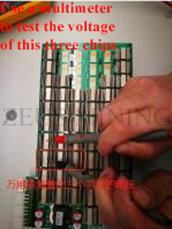
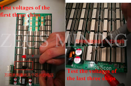
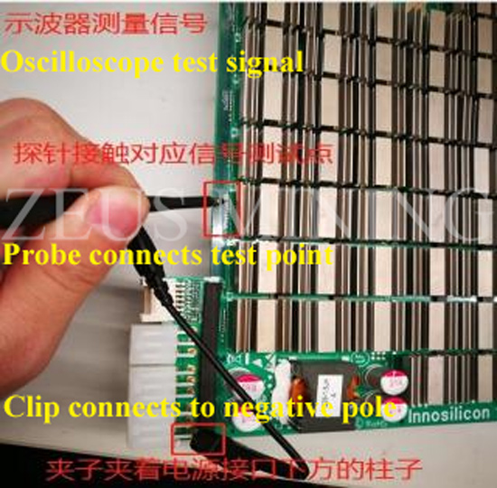
3. E6: N
The voltage of the Nth chip is abnormal.
(1) Use a multimeter to confirm whether the voltage of the chip is abnormal. If the voltage of the chip is too low, detect the SCK signal of the test points of the three chips of this level, and compare the chip with the SCK frequency jitter with other chips of different levels with higher voltage division. Swap. If the SCK signals are normal, replace chip N with other chips of different levels with higher voltage division.
(2) If the problem is with the chip, replace the chip.
4. E7: 0
When E7:0 appears, you need to use maintenance software to locate the problem location, the location method is the same as E0, and test when the program runs to "CRITICAL PLL CONFIGURE ERROR on Board 0 . Begin to Check SPI . "
5. E7: N
Indicates that the chip N does not respond, and you need to replace the chip. The checking method is the same as E0:N.
6. E1: N
The Nth chip lacks a core. If this problem occurs in a large area, submit it to our company for research and development analysis. If only a few hash boards have such problems, replace chip N.
7. E2
The total number of cores on the board is insufficient. At this time, it is necessary to check whether the total voltage of the circuit board is abnormal (refer to the method in E0 error), and if there is no abnormality, it needs to be returned to the factory for repair.
8. E3: N
The softbist error rate of the Nth chip is high. The method is the same as E1:N.
9. E4: N
The pll of the Nth chip is not locked. Check the output CLK of the N-1th chip. If there is no abnormality, resolder the N-1th and Nth chips. If it still can't be solved, replace the Nth chip.
10. E5: N
The temperature of the Nth chip exceeds the standard, replace the chip. If the problem occurs over a large area, you need to check the heat sink. If the problem still cannot be solved, it needs to be returned to the factory.
11. E8
The temperature of the Nth chip exceeds the standard, replace the chip. If the problem occurs over a large area, you need to check the heat sink. If the problem still cannot be solved, it needs to be returned to the factory.
The softbist error rate of the whole board is high, you need to check whether the board voltage and the clock of each chip are abnormal. If abnormal, replace the abnormal chip
If there is no abnormality, it needs to be returned to the factory.。
Ⅴ. Checklist
This checklist is for maintenance reference.
(1) Workmanship inspection
CheckPoint 1. Whether the solder joints of the chip are full and whether there are tin beads
CheckPoint 2. Whether any components fall off
CheckPoint 3. Whether the chip is covered with silicone grease or heat conductive cotton
(2) Check the error message of the software for the pre-glue or post-glue test
CheckPoint 4. Correct identification of chip type
CheckPoint 5. The reading status is normal at the default frequency (Frequency=60Mhz of all chips, Main PLL Lock=1, Temperature, Voltage are within a reasonable range)
CheckPoint 6. Successfully raised to operating frequency (PLL frequency)
CheckPoint 7. The reading status is normal under the operating frequency (Frequency=operating frequency/2, Main PLL Lock=1, Temperature, Voltage of all chips are within a reasonable range)
CheckPoint 8. The error rate of Soft Bist is within a reasonable range (less than 10%)
CheckPoint 9. The test software result is √
CheckPoint 10. The voltage output from the power supply to the hash board is normal (see the indicators of specific models)
CheckPoint 11. The voltage output from the power supply to the control board is 12V ± 10%
(4) Control signal (measured after the hash board is powered on)
CheckPoint 12. EN_CORE=3.3V±10%
CheckPoint 13. RESET=1.8V±10%
CheckPoint 14. START=1.8V±10%
(5) Voltage of chip of hash board
CheckPoint 15. The total CORE voltage should be consistent with the output voltage of the PSU
If the VID setting is unreasonable or ineffective, it will cause abnormal or unstable operation.
If the VID setting does not take effect, check whether the software and hardware programs of the control board are correct.
Innosilicon t2t как разобрать

Пошаговая инструкция как получить 1000 монет WAN и конвертировать их в 200 USDT на Binance
Подключение и настройка Innosilicon
Innosilicon — китайская компания, специализирующаяся на разработке и производстве асик-майнеров для добычи криптовалюты. Если у вас есть асик-майнер от Innosilicon и вы хотите его подключить и настроить, вот общие шаги, которые могут понадобиться:
- Проверьте содержимое упаковки: Убедитесь, что в упаковке находятся все необходимые компоненты, такие как сам асик-майнер, блок питания, кабели и инструкции. Проверьте, что ничего не повреждено или потеряно в процессе доставки.
- Подключите асик-майнер: Следуйте инструкциям, предоставленным производителем, чтобы правильно подключить асик-майнер к электрической сети и к вашему роутеру или сетевому коммутатору с помощью Ethernet-кабеля.
- Настройте IP-адрес: Чтобы получить доступ к интерфейсу управления асик-майнера, вам может потребоваться настроить его IP-адрес. Инструкции по настройке IP-адреса обычно предоставляются производителем вместе с асик-майнером. Вы можете использовать программное обеспечение, предоставляемое производителем, или веб-интерфейс асик-майнера для настройки IP-адреса.
- Настройте пул добычи: Выберите пул добычи, к которому вы хотите присоединиться, и настройте его в асик-майнере. При этом вам потребуется указать адрес пула, порт, имя пользователя и пароль. Информация о пуле обычно предоставляется самим пулом.
- Установите параметры добычи: В зависимости от конкретной модели и типа асик-майнера, вам могут потребоваться дополнительные настройки, такие как скорость хэширования (hashrate), потребляемая мощность и другие параметры, которые вы можете настроить в интерфейсе управления асик-майнера.
- Мониторинг и оптимизация: После подключения и настройки асик-майнера рекомендуется регулярно отслеживать его работу и производительность. Используйте программное обеспечение или веб-интерфейс асик-майнера для мониторинга хэширования, температуры, энергопотребления и других параметров. В случае необходимости вы можете оптимизировать настройки для достижения лучшей производительности или эффективности.
Важно отметить, что конкретные шаги настройки могут варьироваться в зависимости от модели и типа асик-майнера от Innosilicon. Всегда следуйте инструкциям, предоставляемым производителем, и, при необходимости, обратитесь за помощью к службе поддержки Innosilicon.
Какой логин и пароль innosilicon по умолчанию
Информация о логине и пароле по умолчанию для асик-майнеров Innosilicon может различаться в зависимости от конкретной модели и версии прошивки. Однако в большинстве случаев у Innosilicon используются следующие учетные данные по умолчанию:
Логин (Username): root Пароль (Password): admin
Если эти учетные данные не подходят, рекомендуется обратиться к документации, поставляемой с вашим асик-майнером Innosilicon, или обратиться к службе поддержки Innosilicon для получения более точной информации о логине и пароле по умолчанию.
Как сбросить innosilicon t2t до заводских настроек
Для сброса асик-майнера Innosilicon T2T до заводских настроек обычно следуйте этим шагам:
- Подключите асик-майнер к источнику питания и сети, чтобы убедиться, что он включен.
- Найдите кнопку сброса (Reset) на асик-майнере. Обычно она расположена на задней панели или на плате управления. Может потребоваться использование инструмента, такого как штырек или скрепка, чтобы нажать на кнопку.
- Удерживайте кнопку сброса нажатой в течение нескольких секунд (обычно около 5-10 секунд), пока не увидите признаки сброса, такие как загрузочные индикаторы или изменение светодиодных индикаторов.
- После этого отпустите кнопку сброса и дайте асик-майнеру время для перезагрузки и восстановления заводских настроек. Это может занять несколько минут.
После сброса асик-майнер будет находиться в состоянии заводских настроек, и вы сможете выполнить настройку заново, используя логин и пароль по умолчанию или другие указанные в документации производителя.
Как посмотреть температуру innosilicon t2t
Для просмотра температуры асик-майнера Innosilicon T2T можно использовать встроенный интерфейс управления асик-майнером или стороннее программное обеспечение. Вот несколько способов получить информацию о температуре:
- Встроенный интерфейс управления: Подключитесь к асик-майнеру Innosilicon T2T через веб-браузер, используя его IP-адрес. Обычно IP-адрес можно найти в настройках вашего роутера или с помощью программного обеспечения для сканирования сети. После входа в интерфейс управления найдите раздел или вкладку, отображающую информацию о состоянии асик-майнера. Там обычно будет указана текущая температура.
- Программное обеспечение сторонних разработчиков: Существуют сторонние программы, которые могут предоставить дополнительные функции мониторинга и управления асик-майнерами. Некоторые из них позволяют отслеживать температуру и другие параметры работы асик-майнера. Примеры таких программ включают Awesome Miner, CGMiner, BFGMiner и другие. Установите одну из таких программ на свой компьютер, настройте подключение к асик-майнеру Innosilicon T2T и найдите раздел или вкладку, отображающую информацию о температуре.
При мониторинге температуры асик-майнера важно следить за тем, чтобы она оставалась в пределах безопасных значений, указанных производителем. Если температура превышает рекомендуемые значения, может потребоваться настройка системы охлаждения или другие меры для предотвращения перегрева.